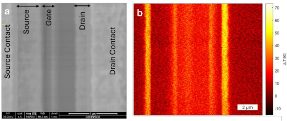
(A) SEM image and (B) Temperature map of the device under test
Invention Summary:
It can be difficult to measure thermal properties at the nanoscale on operating microelectronics in a nondestructive, non-contact and real-time manner. The lack of such nanoscale thermal metrology tools affects quality control in modern microelectronics and impedes rational electro-thermal design of semiconductor devices.
Rutgers researchers have developed an innovative technique that leverages modified commercial Scanning Electron Microscopes (SEM) to provide subsurface temperature mapping and thermal resistance measurements on microelectronic devices in-operando and in real-time. This method enables the construction of a three-dimensional (3D) map with spatial resolutions of less than 3 nm and time resolutions limited only by the readout electronics to the 10 - 100 picosecond level. It utilizes the SEM beam as a nanoscale probe that scans the device surface to detect changes in local electrical resistance and utilizes this information to probe temperature and thermal resistance. Extensive proof-of-concept experiments have been conducted on commercial microelectronic devices. .
Market Applications:
Advantages:
Intellectual Property & Development Status: Provisional application filed. Available for licensing and/or research collaboration. For any business development and other collaborative partnerships, contact: marketingbd@research.rutgers.edu
